
Nanotechnology Fellows Program
Research Projects
Energy Materials Analysis for Additive Manufacturing by Selective Laser Melting
Selective laser melting (SLM) is an additive manufacturing (i.e. 3D printing) technique used to make metal parts with unique geometries which cannot be achieved with traditional manufacturing. In order to make energy devices (e.g. photovoltaics, thermoelectrics, etc.) with SLM, semiconductor materials must be prepared into micro/nanoparticle powders which can be laser melted. This project entails characterizing the thermoelectric material powders for additive manufacturing processes. Preliminary work revealed a need for tuning starting powder morphology and particle size distribution to control flow and spreading characteristics. Particle size distribution, morphology, and packing density will be analyzed with image analysis. Students will analyze spreadability and packing density with optical and scanning electron microscope imaging and subsequent image analysis. The analysis will determine the presence, quantity, size and density of defects (gaps in particle packing continuity). The project will establish a relationship between powder characteristics (particle size distribution, morphology, flow capability, and packing) and the ability to spread continuous layers of uniform thickness. This project entails using microscopy techniques and image analyses.
Carbon Nanoparticle Inks for Inkjet Printing Applications
Inkjet is a widely used technology in consumer and industrial printing applications. Recently it has shown utility as an additive manufacturing technique for creating large arrays of functional devices such as thin and flexible electronics, photovoltaics, thermoelectrics, and chemical sensors. Inkjet is advantageous when mass production and compatibility with a wide variety of materials and substrates are desirable. Functional material particles are dispersed into a liquid carrier to create a printable ink. In this case, the particles are carbon nanospheres synthesized from biochar, an agricultural waste product. For an ink to be printable, the dispersed particles must be stable from settling and agglomeration. This project will use dynamic light scattering to determine the stability of carbon nanoparticles in several aqueous solutions.
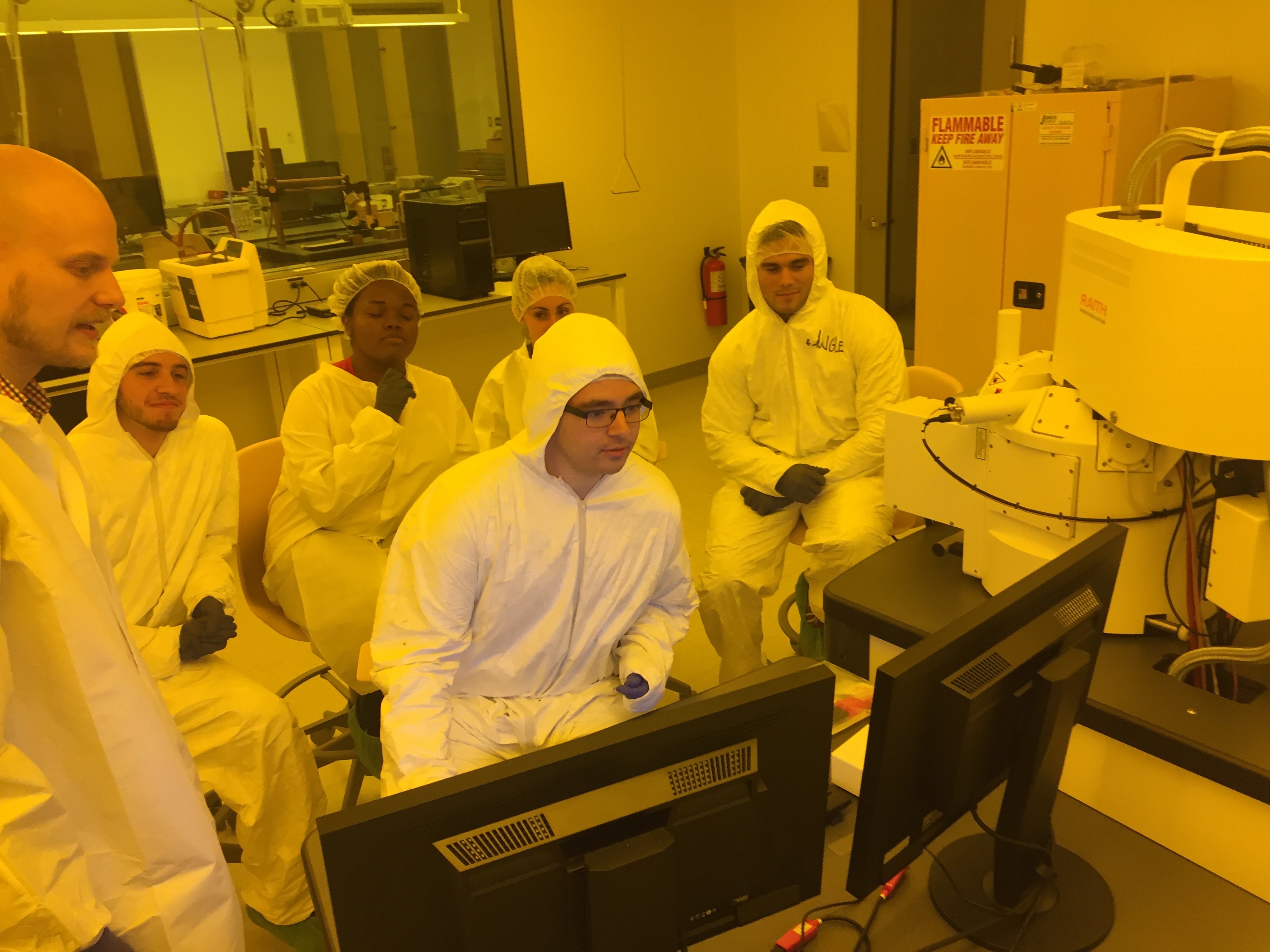
Electrical Characterization of 2D Materials
2D materials are atomically thin and have attracted great interest because of their exceptional electrical and optical properties. They demonstrate all different class of materials, such as conductors, semiconductors, and insulators. Hence, they are being considered for a wide range of applications including optoelectronics. Transparent conductive sheets such as graphene are particularly attractive for their application as a contact material in the smart phone industry. Semiconductor types such as tungsten disulfide are attractive for light generation and absorption applications such as LEDs or solar cells. In this project we will use electron beam lithography to pattern 2D material such as graphene or tungsten disulfide. We will also use thermal evaporator, to define electrical contact, and electrical probing to characterize their electrical and optical properties.
High Contrast Gratings for Guiding Light
Diffraction gratings are optical components used to separate light into its fundamental wavelengths. They are transmissive or reflective. As a white light transmits through or reflects off the grating, the grooves break up the light into its elemental wavelengths with great precision and effectiveness. A real-life example of diffraction grating is a CD. We use diffraction-based encoders in security, telecommunications, semiconductor processing industries, or in renewable energies. Diffractive optics (holographic optics) is the product of the era of information technologies. Creation of diffraction grating requires advance technologies used in the integrated circuit industry. One of the most recent and exciting applications of diffraction is in virtual reality where they help to extract an image to an optical waveguide. In this project, we will go through the lithographical process flow used in semiconductor industry to achieve precise diffraction gratings to guide light.